(China (Mainland))

Product Summary
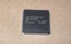
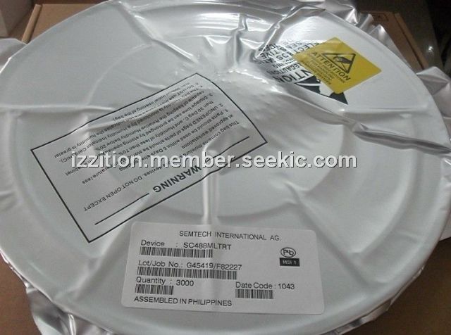
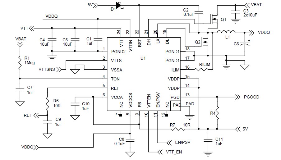
The SC488MLTRT is a combination switching regulator and linear source/sink regulator intended for DDR1/2 memory systems. The purpose of the switching regulator SC488MLTRT is to generate the supply voltage, VDDQ, for the memory system. It is a pseudo-fixed frequency constant on-time controller designed for high effi ciency, superior DC accuracy, and fast transient response. The purpose of the linear source/sink regulator is to generate the memory termination voltage, VTT, with the ability to source and sink 2.8A peak currents.
Parametrics
SC488MLTRT absolute maximum ratings: (1)Thermal Resistance Junction to Ambient θJA: 29 ℃/W; (2)Operating Junction Temperature Range TJ: -40 to +150 ℃; (3)Storage Temperature Range TSTG: -65 to +150 ℃; (4)Peak IR Refl ow Temperature, 10s - 40s TPKG: 260 ℃; (5)ESD Protection Level VESD: 2 kV; (6)TON to VSSA: -0.3 to +25.0 V; (7)DH, BST to PGND1: -0.3 to +31.0 V; (8)BST, DH to LX: -0.3 to +6.0 V; (9)LX to PGND1: -2.0 to +25.0 V.
Features
SC488MLTRT features: (1)External RSENSE in Series with Low-Side FET; (2)Cycle-by-Cycle Current Limit for VDDQ; (3)Digital Soft-Start for VDDQ; (4)Analog Soft-Start for VTT/REF; (5)Smart Over-Voltage VDDQ Protection; (6)Combined EN and PSAVE Pin for VDDQ; (7)Over-Voltage/Under-Voltage Fault Protection; (8)Power Good Output; (9)Separate VCCA and VDDP Supplies; (10)VTT/REF Range = 0.75V – 1.5V; (11)VTT Source/Sink 2.8A Peak; (12)Internal Resistor Divider for VTT/REF; (13)VTT is High Impedance in S3; (14)VDDQ, VTT, REF are Actively Discharged in S4/S5; (15)24 Lead MLPQ (4x4 mm) Lead-Free Package; (16)Product Is Fully WEEE and RoHS Compliant.
Diagrams
 |
 SC4808B-1 |
Other |
|
Data Sheet |
Negotiable |
|
||||